Flash Memory Goes 3D

As traditional NAND flash storage technology approaches the end of the line, chipmakers Intel Corp. and Micron Technology jointly began investigating new approaches to cell design that could be leveraged to dramatically improve storage capacity, performance and reliability. Two-dimensional planar scaling of flash memory cells was on a Moore's Law path to obsolescence, so the semiconductor leaders formed a joint development project about a decade ago to study floating gate cell technology and how it could be scaled.
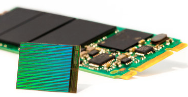
The result, the partners announced this week, is 3D NAND cell technology they will leverage to produce new flash storage products like a flash drive the size of a gum stick capable of storing 3.5 TB of data.
The partners said this week they are entering initial production on 3D NAND flash components that are sampling now. Both chipmakers said they expect to start offering flash memory products based on 3D floating gate cell technology in the second half of 2015.
Three-dimensional NAND flash technology stacks layers of data storage cells as a way to essentially triple storage capacity. The architecture translates into higher cell densities and more storage in a smaller package.
The partners said the NAND flash drives now sampling include 32 layers crammed inside a 3D NAND cell. Given the size reductions, the partners are primarily targeting the mobile market, but the advance is sure to make its way into solid-state storage systems and enterprise flash storage deployments.
The "stunning densities" were achieved using a floating gate cell approach, according to Giri Giridhar, Intel's vice president of non-volatile technology development. Giridhar said the NAND flash components from Intel and Micron that are currently sampling are the first to use floating gate cell technology in a 3D NAND. Floating gate cell technology "was a key design choice" to boost memory performance, Giridhar said Thursday (March 26).
Flash cells were stacked vertically in layers to create multilevel cells that fit within a standard chip package. The result, the partners said, is a gum stick-sized SSD with more than 3.5 TB of storage. A standard 2.5-inch SSD based on the technology could provide as much as 10 TB of storage, the partners said.
Moreover, triple-level cell designs in which individual cell dimensions could be scaled up, then stacked, could be used for datacenter storage. "We are scaling vertically, so we can stack up more cells," Giridhar stressed.
The first generation 3D NAND has already topped the cost per GB rating of traditional planar NAND technologies. Hence the cell densities achieved so far could allow the technology to make inroads in the storage infrastructure built around mobile technologies. Later generations of 3D NAND will likely be deployed as part of datacenter storage infrastructure, the partners predicted.
For now, Intel officials claimed 3D NAND has achieved price parity with spinning disk storage.
The partners said initial production of the 3D NAND chips has begun at a joint flash technology wafer fab in Singapore. They said a 256-GB multiple-level cell chip along with a 384-GB triple-level cell would enter full production by the end of this year. The 256-Gb version is sampling now.
Both chipmakers are developing individual SSD product lines based on the 3D NAND technology. Those products are expected to hit the market in the next year. No products were announced this week.
Related
George Leopold has written about science and technology for more than 30 years, focusing on electronics and aerospace technology. He previously served as executive editor of Electronic Engineering Times. Leopold is the author of "Calculated Risk: The Supersonic Life and Times of Gus Grissom" (Purdue University Press, 2016).


