Sandia Partners with National Labs to Develop Energy-Efficient AI and Computing Tech
ALBUQUERQUE, N.M., Jan. 6, 2025 -- Sandia National Laboratories is collaborating with other research institutions to head off a potential future energy crisis that could be driven in part by artificial intelligence.

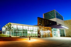
The Center for Integrated Nanotechnologies, pictured here, is one of five Department of Energy Nanoscale Science Research Centers teaming up to help make computer chips more energy-efficient. Credit: Randy Montoya.
“We face an unprecedented microelectronics energy efficiency challenge,” Sandia’s Jeffrey Nelson said. “Computing alone is projected to consume a significant portion of the total planetary energy production within a decade.”
To meet future needs, the Department of Energy Office of Science recently announced the creation of three new Microelectronics Science Research Centers. One center, the Microelectronics Energy Efficiency Research Center for Advanced Technologies, or MEERCAT, will focus on energy efficiency, exploring solutions that bridge sensing, edge processing, artificial intelligence and high-performance computing. Sandia will be a founding member of MEERCAT and will lead one of the eight energy efficiency-related research projects within the center.
The other two centers will work on resilience in extreme environments, including high-radiation, cryogenic and high magnetic field environments.
“Our center will provide industry with new, higher performance options for energy-efficient computing,” said Nelson, the principal investigator for the Sandia-led project.
Sandia is also partnering on two projects led by other laboratories: one on energy efficiency with Lawrence Berkeley National Laboratory and another on extreme environments with Los Alamos National Laboratory.
AI is a major factor in rising energy demand because it uses more energy than conventional computer algorithms and has seen a surge in popularity within homes and workplaces. Along with the growth of other energy-intensive technologies like quantum computing and advanced sensors, this has created an urgent need for more efficient technologies.
The three new research centers will provide a total of $179 million for 16 multidisciplinary, fundamental research projects lasting up to four years. They are funded through DOE’s Office of Science and authorized by the Micro Act, passed in the CHIPS and Science Act of 2022. This legislation has invested billions of dollars through multiple agencies to help companies build new plants for advanced semiconductors in the U.S. It also funds fundamental research to advance the technologies these future factories will produce.
“We are working with companies to understand their problems and pulling experts together from across the DOE to solve these problems quickly,” Nelson said.
Project Seeks to Unleash Potential of New Materials
When the Energy Department announced its plan to form Microelectronics Science Research Centers in May 2024, Nelson reached out to a familiar team.
Two years earlier, a group of directors and experts from DOE’s five scientific user facilities, the Nanoscale Science Research Centers, had started holding regular, collaborative discussions.
“We met every two weeks for two years,” Nelson said. “We discussed our collective resources and how we can work together to achieve national priorities.”
Nelson is the director of one of these Office of Science user facilities, the Center for Integrated Nanotechnologies, which is jointly operated by Sandia and Los Alamos national laboratories. The other four user facilities: the Center for Nanoscale Materials, the Center for Functional Nanomaterials, The Molecular Foundry and the Center for Nanophase Materials Sciences are spread across the country, each co-located at a national lab.
The team agreed that by working together they could advance new materials to make computing more powerful and energy-efficient.
Researchers had already found that materials like molybdenum disulfide, gallium arsenide and even diamond may be better than silicon for certain aspects of computing. In theory, computer chips made from one of these alternative materials might be far more energy-efficient and could solve the looming energy crisis.
“They’re very promising,” Nelson said.
But the task of taking any of these materials, perfecting them in a lab, learning how to mass produce them and then building a factory to make chips from them while competing against an established silicon industry and supply chain, the team agreed, felt daunting at best.
Taking a different route, the group of lab leads and other collaborators proposed a project entitled “Nano-Scale Research Center for Heterogeneous Integration Platforms.” This project would aim to leverage the existing infrastructure and expertise of the DOE user facilities and partnering institutions and develop ways to insert new materials into standard silicon fabrication processes.
Now greenlit with DOE’s recent announcement, the project will bring together resources from all five Nanoscale Science Research Centers. It will also include researchers from Fermi National Accelerator Laboratory, the Massachusetts Institute of Technology and MIT Lincoln Laboratory.
They will build on previous research in what scientists call heterogeneous integration. This means using many kinds of materials to make computer chips, all monolithically integrated into a silicon backbone. The tricky part is to ensure electrons and information flow seamlessly between different materials.
Sandia and its collaborators are aiming for breakthroughs that could help industry create much more energy-efficient computer chips.
“By collaborating across multiple national laboratories and universities, our goal is really to accelerate the innovation discovery process and make a positive impact on economic and national security,” Nelson said.
About Sandia National Laboratories
Sandia National Laboratories is a multimission laboratory operated by National Technology and Engineering Solutions of Sandia LLC, a wholly owned subsidiary of Honeywell International Inc., for the U.S. Department of Energy’s National Nuclear Security Administration. Sandia Labs has major research and development responsibilities in nuclear deterrence, global security, defense, energy technologies and economic competitiveness, with main facilities in Albuquerque, New Mexico, and Livermore, California.
Source: Sandia National Laboratories


